Research
CHARACTERIZATION OF CIS/CDS THIN-FILM PHOTOVOLTAICS BY
X-RAY PHOTOELECTRON SPECTROSCOPY
Photovoltaic power sources are the best opportunity to provide energy for the world of tomorrow so it is important to understan the surface, electrical and photo-induced properties of them in order to increase their efficiencies. Currently used materials in
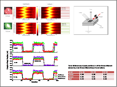 photovoltaic manufacturing technology are crystalline silicon, CdTe (cadmium telluride), amorphous and nanocrystalline silicon, CIS (copper indium diselenide) and CIGS (copper indium gallium selenide).This research focuses only on the CIS cells, which contains a CdS layer on top. X-ray photoelectron spectroscopy (XPS) analyses were performed to investigate CIS/CdS based thin-film photovoltaics. The main objective of the research is to show the different elemental responses as shifts of the XPS Cd 3d, Cu 2p, S 2p and In 3d peak position under photoillumination with three different lasers. Furthermore, electrical charging properties of CIS/CdS thin film are studied with externally applied squarewave pulses Dynamic XPS. Results will be presented with an ultimate aim of better understanding of the roles of defects affecting the performance of CIS devices.
INVESTIGATION OF TRIBOCHEMICAL INTERACTION BETWEEN POLYTETRAFLUOROETHYLENE AND SiO2/Si SURFACES: WETTABILITY
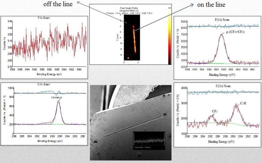
This work focuses on the investigation of the tribochemical interaction between thermally-oxidized and variously treated (with deionized water/0,1M HCl/0,1M NaOH) silicon surfaces and polytetrafluoroethylene, and the potential effects of this interaction on the wettability of SiO2 surfaces. A simple rig was designed to generate a rubbing motion between the surfaces and PTFE tip with an approximate angle of 45° employing also an inclination along the motion in order to bring about a gradual tribochemical interaction. After some patterns were sketched on the SiO2 surface using the PTFE, the nature of the interaction was characterized by X-Ray Photoelectron Spectroscopy (XPS) and Scanning Electron Microscopy (SEM). Moreover, in order to characterize and monitor the changes in wettability of surfaces, contact angle measurements were also carried out. In addition to XPS and SEM results illustrated that PTFE could indeed be transferred onto SiO2 surfaces even in the case of the application of the friction at relatively small forces, contact angle measurement results showed that the hydrophobicity of the SiO2 surfaces could be significantly increased depending this PTFE transfer, which might also depend on the kind of treatments on the SiO2 surfaces and the density of PTFE transferred onto the surface.
INDUCING N-DOPING TO TITANIUM DIOXIDE BY CHEMICAL ROUTES AND CHARACTERIZATION BY X-RAY PHOTOELECTRON SPECTROSCOPY
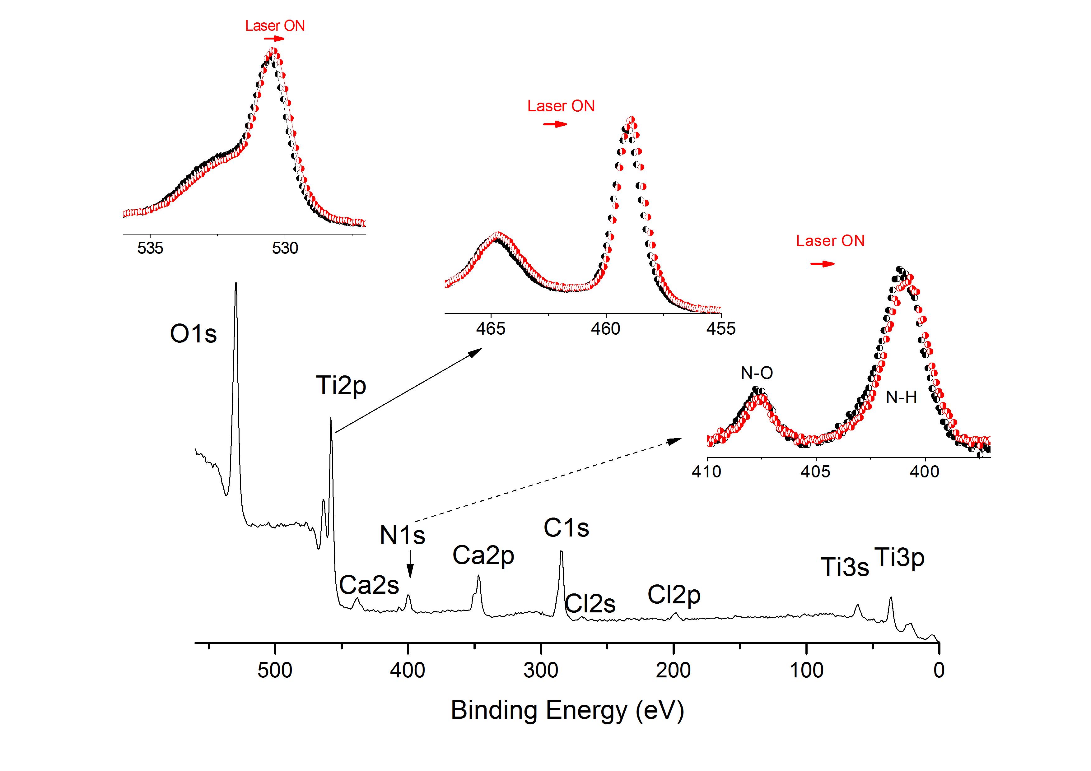
Titanium dioxide is an important material with significant photocatalytic activity in the UV region, which has also been utilized for other important applications ranging from sensors to photovoltaics. The material is a naturally n-doped one due to the presence of O-deficiencies irrespective of its preparation techniques, it can acquire photocatalytic activity in the visible region after introduction of suitable dopants into some interstitial or substitional sites using physical, chemical and electrochemical routes… In the seminal paper published by Asahi et. al., N-doping was proposed and demonstrated to be an efficient way both for introducing photocatalytic activity in the Visible range as well as making the material p-doped[1]… We have tried to induce N-doping into various titanium dioxide samples by sol-gel methods or just dipping them into ammonia solutions, and have utilized XPS to characterize the changes both in terms of chemical composition as well as photo-electrochemical response.
MECHANICALLY ASSISTED GOLD PARTICLES DEPOSTION BY GALVANIC DISPLACEMENT ON SILICON SURFACES AND CHARACTERIZATION BY X-RAY PHOTOELECTRON SPECTROSCOPY
The electrotless deposition of metallic nanoparticles onto semiconducting surfaces by galvanic displacement method has applications ranging from electronic devices to chemical sensors. For the spontaneous deposition of gold onto silicon surfaces by galvanic displacement, a gold (III) salt is needed, which will be reduced to metallic state on the surface by electrons coming from the silicon. It is also known that presence of defects, mechanical attritions, scratches, etc. enhance this process. For this purpose, we have created some parallel columnar attritions using a metal tip on n- and p-type silicon wafers. Deposition and presence of metallic gold on or around the attritions have been examined using optical and electron microscopic (SEM) techniques, as well as X-ray photoelectron spectroscopic (XPS) mapping. Presence of gold deposition on or around the attritions created on p-type silicon surfaces has been confirmed by XPS. However, when an oxide layer has been introduced by thermal means, no significant deposition has been observed.